What happens to the electronic surface of a topological material when it touches a magnet? And can we use those changes to turn spin into an electrical signal more efficiently? In a new study led by Masayuki Ishida, we tackled these questions by placing iron directly on a thin film of alpha-tin (α-Sn). Our results point to the far side of the tin film, where it meets the underlying semiconductor, as the main site of conversion. By adjusting the film thickness, we achieved one of the highest spin-to-charge conversion values reported at room temperature. The paper was selected as an Editors’ Suggestion in Physical Review B.
What direct contact with a magnet changes
Electrons carry both electric charge and a property called spin, which makes them behave like tiny magnets. Spintronics uses spin to carry information. To read that information with an ordinary electronic circuit, we need a way to turn a flow of spin into an electrical signal. In α-Sn, this can happen through topological surface states. In these states, the direction an electron moves is linked to the direction of its spin, allowing an incoming flow of spin to generate an electrical current.
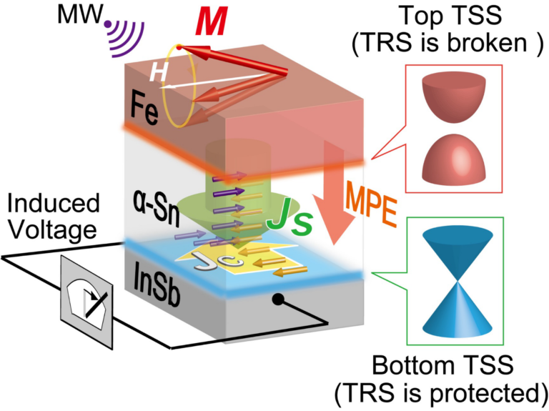
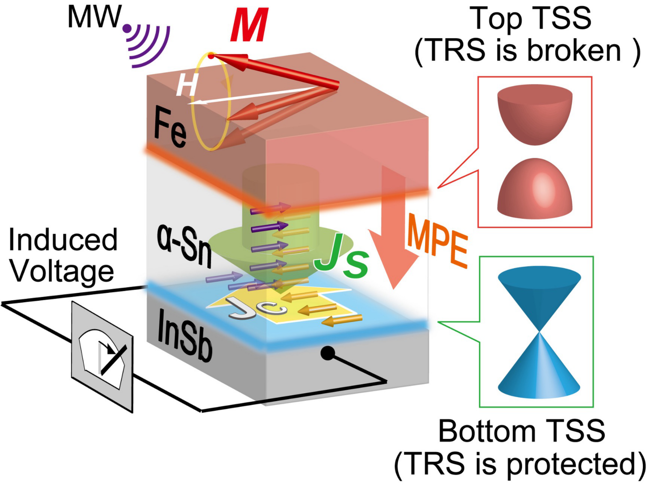
Putting a ferromagnet such as iron directly against α-Sn gives us a way to inject spin. The same contact also changes the electronic states we want to use. Earlier studies often placed a thin spacer between the magnet and the topological material to protect those states. Two questions remained open for structures with direct contact. How does the magnet reshape the surface states on both sides of the film? And how can we use those changes to improve conversion?
Why 25 nanometers made a difference
We grew α-Sn films of several thicknesses on indium antimonide (InSb), then deposited iron directly on top. Using microwaves, we drove the magnetization of the iron into motion, which pumped spin into the tin. The iron’s magnetic motion lost energy fastest in the 25-nanometer film, indicating stronger spin transfer out of the iron. In that sample, we also measured a steady voltage that increased with microwave power. The estimated inverse Edelstein length, a measure of how effectively an interface converts spin flow into current, was −3.1 ± 1.0 nm. Its magnitude ranks among the largest reported at room temperature, and its sign indicates the direction of the generated current for a given spin orientation.
Our calculations explain why thickness matters. At the iron contact, strong interactions with iron largely suppress the topological surface states. On the opposite side, where α-Sn meets InSb, a surface state survives, although iron’s magnetic influence still alters it. In thinner films, that influence is stronger at the far interface. In thicker films, more of the injected spin signal fades before it reaches that interface. At 25 nanometers, the film balances these two effects. The direction of the measured voltage also supports the interpretation that conversion takes place mainly at the α-Sn/InSb interface.
Designing both interfaces for room-temperature spintronics
In our structure, one interface injects spin and the other converts it into an electrical signal. Controlling the film thickness lets us engineer the surface state at the far interface while keeping it close enough to receive spin from the iron. This approach achieved strong room-temperature conversion with a simple stack and no spacer between iron and α-Sn. It offers a design principle for future low-power spintronic devices, including circuits that read magnetic information as a voltage.
For more details: