From the fundamental point of view, probing spin dynamics phenomena at an ultrafast time scale potentially reveals the underlying mechanisms of various strong magnetic couplings in magnetic materials, such as exchange interactions and spin-orbit interactions. Practically, controlling the magnetization of ferromagnets on a subpicosecond (sub-ps) time scale would enable low-power-consumption and ultrahigh-speed operation of new spin-based electronic devices at THz frequencies, which is beyond the limitations of the present CMOS circuitry.
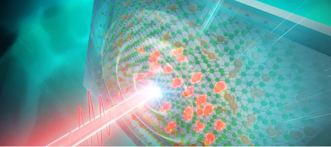
The answer is, extremely fast! – ranging from several femtosecond (=10^-15 second) to 100 picosecond (=10^-12 second), up to date. The upper limit of this time scale is set by the magnetic interaction energy (the energy scale that spins interact), or s,p-d exchange interactions (the energy scale that spins interact with carriers), which establish the ferromagnetic order. In general, these energies in magnetic materials (metals, semiconductors, insulators) are in an order of ~ 1eV, which corresponds to a time limit of 1 fs according to the Heisenberg uncertainty principle.
How to instantly magnetize a magnetic material? Thus far, ultrafast enhancement of magnetization requires instant pumping of a large amount of carriers (~10^20 cm^-3) into the d or f orbitals, in the case of ferromagnetic metals, or into the s, p orbitals, where these carriers interact with the localized spins like in the case of ferromagnetic semiconductors. Most of the cases, this was implemented by employing fs-pulse lasers with strong fluences to excite magnetic materials. When the photon energy coincides with a resonant transition between different bands, the laser pulses excite carriers into d or f-orbital spin-polarized bands.
So, what was the problem? It is highly desired that the same ultrafast spin dynamics can be implemented in the present CMOS circuitry due to its mature device technologies, the abilities of accurate control at the nanoscale and very large-scale integration. Unlike optical pumping, however, electrical gating, the basic operation in CMOS, can never largely change the carrier density nor cause band-to-band transitions in the ultrafast time scale.
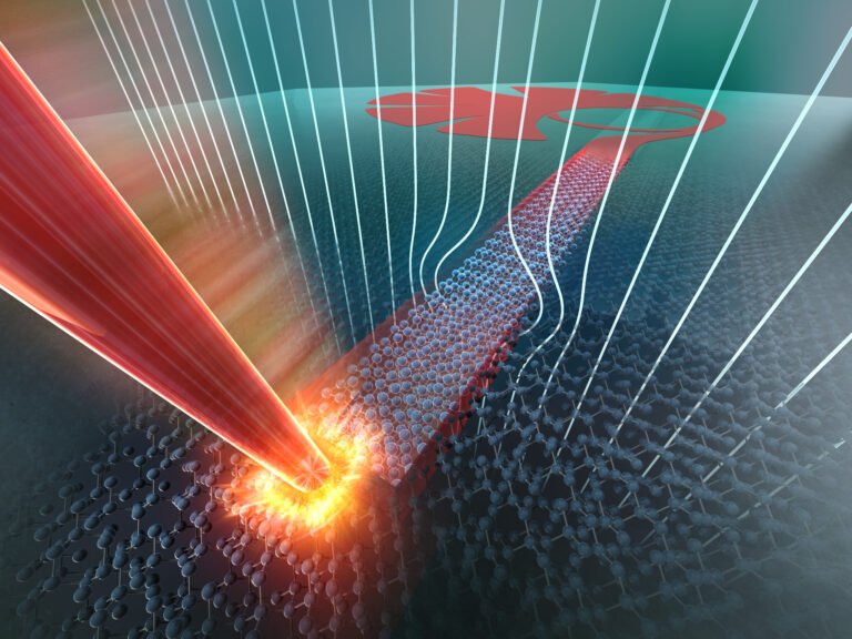
How do we solve the problem? In our newest publication [Adv. Mater. 202301347 (2023)], we demonstrates a new method for sub-ps magnetisation manipulation, called wavefunction engineering, in which we control only the spatial distribution (wavefunction) of s (or p) electrons and require no change in the total carrier density. Using a ferromagnetic semiconductor (FMS) (In,Fe)As quantum well (QW), we observe instant enhancement, as fast as 600 fs, of the magnetisation upon irradiating a femtosecond (fs) laser pulse (see Fig 1 below).

The key factor of our successful demonstration is the use of an (In,Fe)As (10 nm)/InAs (5 nm) bilayer QW structure, as shown in Fig. 2, where (In,Fe)As is a ferromagnetic semiconductor (FMS) and InAs is a nonmagnetic semiconductor. In (In,Fe)As, which is the first carrier-induced n-type FMS, electron carriers possess coherence lengths as long as 40 nm. Therefore, a thin (In,Fe)As/InAs bilayer structure forms a surface QW where the electron carrier WF is extended throughout the bilayer. The important feature of this two-dimensional (2D) ferromagnetic structure is that magnetic properties such as the Curie temperature (Tc) are determined by the spatial overlap between the WF and the local spins (Fe) in (In,Fe)As. Thus, by controlling the WF peak position and shape, one can effectively change the magnetic properties of the (In,Fe)As/InAs QW without pumping extra carriers into the system. In this new method, the power consumption is extremely low, which was demonstrated to be one million times less than the conventional method, and the operating speed can exceed the unprecedented ps limit because it involves no carrier accumulation process other than moving the electron WF back and forth only a few nanometres within the QW. Indeed, our analysis shows that 2D electron WFs in the FMS QW can be rapidly moved by a photo-Dember electric field formed by an asymmetric distribution of the photocarriers, inducing instant enhancement of the magnetization.
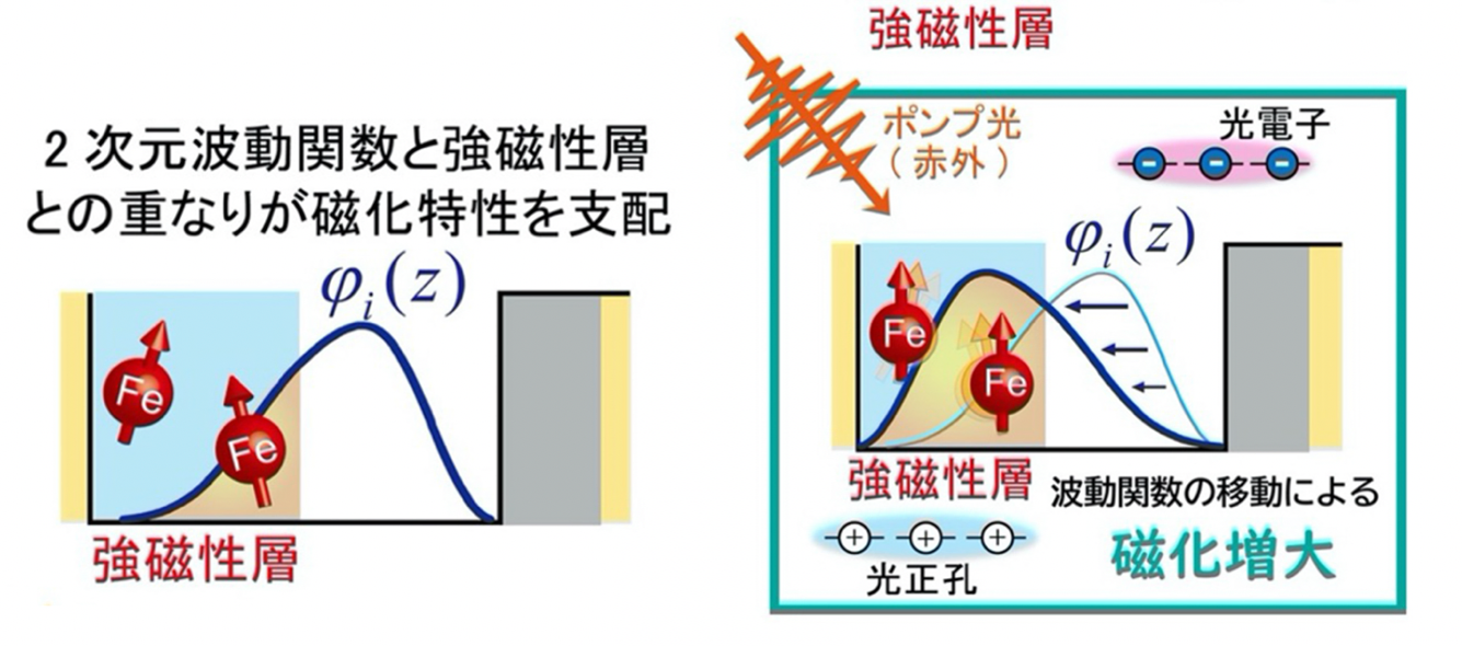
What are the future aspects? The ability to control the magnetisation of a magnetic material on the sub-ps time scale is a remarkable feature of a ferromagnetic QW, where the high coherency of the itinerant carriers enables ultrafast control of their distribution via the WFs.Schemes to control the carrier WFs are certainly not limited to optical pumping and can also be performed by applying a gate voltage in transistor structures. Because there is no need to accumulate extra charge carriers in the ferromagnetic QW, the gate capacitance C can be reduced as much as possible through appropriate design of materials and devices. Therefore, the gating operation speed, which is limited by the RC constant, where R is the wiring resistance, can be sub-ps. Because the relevant time of spin-charge interactions is as fast as the sub-ps scale, as experimentally presented in this work, electrical control of ferromagnetism utilizing WF engineering may potentially lead to ultrafast and scalable electronic devices in the future.
Ref: Le Duc Anh, Masaki Kobayashi, Takahito Takeda, Kohsei Araki, Ryo Okano, Toshihide Sumi, Masafumi Horio, Kohei Yamamoto, Yuya Kubota, Shigeki Owada, Makina Yabashi, Iwao Matsuda, Masaaki Tanaka, Ultrafast Subpicosecond Magnetization of a 2D Ferromagnet. Advanced Materials, 2301347 (2023).
DOI: https://doi.org/10.1002/adma.202301347 (Open access)


