Superconductors can carry electrical current with zero resistance, offering an ultra-efficient platform for next-generation electronics and quantum technologies. Meanwhile, “topological” materials, whose electrons behave in unusually robust ways, are promising building blocks for fault-tolerant quantum devices. However, combining the two cleanly is highly challenging; standard nanofabrication methods can roughen or damage delicate crystals, and even tiny imperfections at the interface can degrade performance.
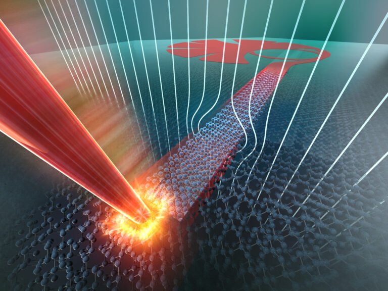
Our group has demonstrated a surprisingly simple solution. They used a focused laser beam as a nanoscale “pen” to locally transform a topological tin film into a superconducting region without physically cutting, etching, or bombarding it. The team worked with α-Sn (alpha-tin), a topological Dirac semimetal thin film epitaxially grown on an InSb substrate; they used localized laser heating to trigger a phase change only where the beam was aimed, converting the α-Sn into β-Sn (beta-tin), a well-known superconducting metal. In other words, they can make superconducting nanostructures of almost any shape directly in a topological thin film. This creates a high-precision α-Sn/β-Sn in-plane heterostructure on a single wafer.
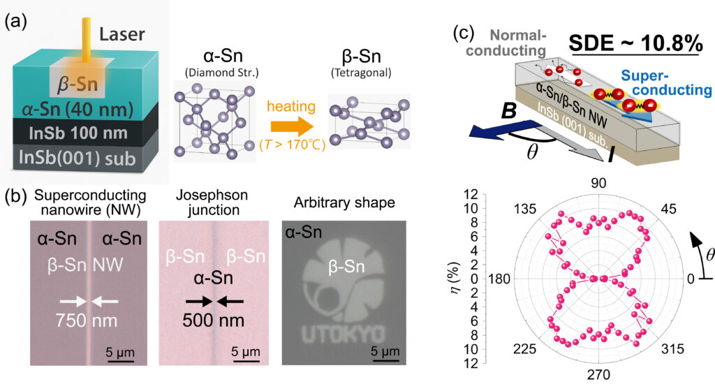
Figure. (a) Schematic image of α-Sn/β-Sn planar nanostructures fabricated by laser irradiation (left panel). Phase transition from topological Dirac semimetal α-Sn to superconducting metal β-Sn induced by local heating by irradiating a laser beam (right panel). (b) Optical microscopy image of a 750 nm-wide β-Sn nanowire (white) embedded in a α-Sn matrix (gray), β-Sn/α-Sn/β-Sn Josephson junction structure with a 500 nm-wide central α-Sn region (gray), and arbitrarily designed β-Sn patterns (white). All these patterns were formed by laser irradiation, demonstrating high flexibility and compatibility with standard nanofabrication techniques. (c) Superconducting diode effect (SDE) in a laser-induced β-Sn nanowire (NW) embedded in α-Sn, where the NW exhibits superconductivity in one current direction and normal-conductivity in the opposite one. The SDE efficiency (η) reaches maximum of 10.8% when magnetic field B is applied in-plane and deviated from the current I by an angle θ = 45°, 135°, 225°, 315°.
This approach is especially attractive for future devices because of its quality and gentleness. Since the method uses heat instead of physically invasive processing, the resulting superconducting β-Sn regions have atomically smooth surfaces and nearly single-crystal quality over large areas. These properties are critical for sensitive superconducting and quantum circuits. This approach is also mask-free and potentially scalable, suggesting a practical, lower-cost path toward manufacturing complex superconducting patterns.
To demonstrate the effectiveness of this “laser writing” technique, the research team fabricated β-Sn nanowires just hundreds of nanometers in width and observed a striking phenomenon: a superconducting diode effect, where the nanowires allow current to flow without any resistance (a superconducting current) in one direction but remain resistive-like normal conductors-in the other. Remarkably, the device exhibited this effect even without an applied magnetic field; the diode device showed superconducting transport with zero resistance in one current direction while showing normal transport with non-zero resistance in the opposite current direction. By adjusting the direction of an applied magnetic field, the team achieved a maximum rectification ratio of 10.8%, demonstrating controllable and directional superconducting behavior in a compact nanostructure.
This work is more than just a clever fabrication trick; it provides a new toolkit for building superconducting quantum devices and quantum circuits that require exceptionally clean and well-defined interfaces. Because the platform uses two phases of the single element (tin) to integrate topological and superconducting functionalities, it provides a direct and customizable approach to exploring topological superconductivity and designing device architectures that were previously difficult to produce without causing damage to the material.
Papers
Journal: Advanced Materials
Title: Non-Destructive Laser Nanopatterning of Superconducting Heterostructures in Topological Sn Thin Films
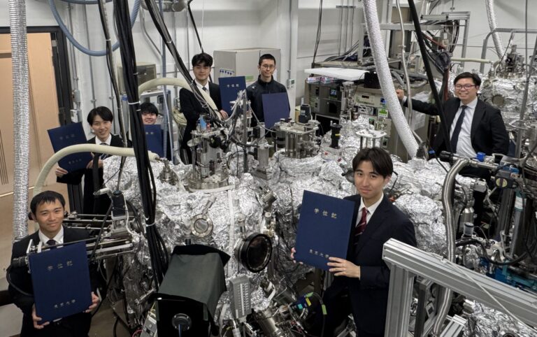
Authors: Le Duc Anh, Takahiro Saeki, Keita Ishihara, Daiki Nishigaki, Hideki Maki, Masaaki Tanaka
DOI: 10.1002/adma.202512571