Fe-based Ferromagnetic Semiconductors and Devices Applications
Over the past 50 years, the development of information and communication technology (ICT) has been led by the miniaturization of semiconductor integrated circuits, following the Moore’s law. In transistors nowadays, the source and drain electrodes are separated only by a distance of a few atoms, where the quantum tunneling effect becomes dominant. This enhances the leaking currrent in transistors even when they are inactive, degrades the devices performance, and the power consumption of ICT devices are skyrocketing. Facing these physical limitations, there is a strong demand for dramatic advances in existing semiconductor materials.
Spintronics, which aims to integrate a spin degree of freedom into conventional electronics, has been one of the most active fields in the development of electronics and solid state physics in the recent decades. In particular, introducing ferromagnetism into mainstream semiconductors is of fundamental importance and great interest, because it provides the ability to control the output of principal devices such as transistors, diodes, or lasers by manipulating both the “charge” and “spin” of an electron. This brings about new devices with novel functionalities such as non-volatility, non-reciprocity and reconfigurability, which are essential for paradigm-shifting electronics beyond the present scalability limit and many possible applications in quantum computation.
To make a semiconductor ferromagnetic is very challenging. The conventional approach is to dope a certain amount (several percentages) of magnetic elements into a semiconductor without significantly altering the crystal structure and semiconducting properties of the host material. Several elements that possess d-orbital or f-orbital electrons have been tried as the dopant, which are usually transition metals such as Mn, Co, Fe or rare-earth metals such as Cs, Eu,… Thus far, significant success has been achieved in III-V compound semiconductor GaAs doped with Manganese (Mn), in which carrier-induced ferromagnetism and important phenomena such as tunneling magnetoresistance were demonstrated. The Mn-based III-V ferromagnetic semiconductors (FMSs) are the prototype materials for new proof-of-concept devices such as spin-transistors, spin-lasers, and new physics such as electrical-controlled magnetism, which are being widely extended to other classes of materials. However, towards a realization of practical spin-electronics, Mn-based FMSs also possess severe shortcomings: (1)Their Curie temperature (TC) is much lower than room-temperature (< 200 K). (2) Only p-type FMSs are available, because Mn dopants act as very good acceptors. To obtain both p-type and n-type room-temperature FMSs, which requires a fundamentally different approach beyond Mn-based FMSs, has long been the holy grail pursued by many research groups around the world, including us.

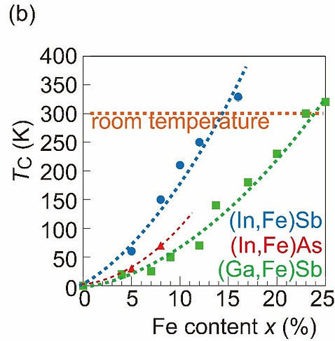
Fig 1. (a) Zinc-blende crystal structure of Fe-doped III-V FMSs and transmission electron microscopy (TEM) images of (Ga,Fe)Sb, (In,Fe)As, and (In,Fe)Sb, respectively. (b) Curie temperature TC as a function of the Fe content x in (In,Fe)Sb, (In,Fe)As, and (Ga,Fe)Sb.
Fe-based narrow-gap III-V ferromagnetic semiconductors
Starting from 2010, we focused our study in developing a new class of FMSs – Fe-based narrow-gap III-V FMSs – which includes (In,Fe)As, (Ga,Fe)Sb, (In,Fe)Sb and (Al,Fe)Sb. We decided to use Fe in III-V semiconductors, because Fe can replace the III-group element in the Fe3+ state, which is electrically neutral (which means it supply neither electron nor hole). By this virtue, we expected that the conduction type (n or p) can be independently controlled, and a larger amount of magnetic elements can be doped while maintaining the stability of the semiconductor crystal structure. Contrary with the traditional belief that high TC is unlikely in narrow-gap semiconductors [T. Dietl et al, Science 287, 1019 (2000)], our results surprisingly proved that these Fe-based narrow-gap FMSs can achieve room-temperature ferromagnetism in both p-type and n-type materials, which are the key features to realize practical semiconductor-based spintronics, and many more unprecedented functionalities as explained below.
-
We realized both p-type and n-type FMSs: We showed that Fe atoms replace the III-sites in these III-V FMSs and act only as localized spins and supply no carriers. Therefore, using molecular beam epitaxy, we have successfully grown the first ever n-type FMSs in (In,Fe)As [APL 101, 182403 (2012)] and later (In,Fe)Sb [APEX 11 (6), 063005 (2018)]. On the other hand, (Ga,Fe)Sb [APL 105, 132402 (2014); PRB 92, 144403 (2015)] and (Al,Fe)Sb [APL107, 232405 (2015)] are p-type. An appealing advantage is that the lattice constants of these FMSs are very closely matched (~6.1Å), which enables the epitaxial growth of their high-quality heterostructures, such as pn junctions (Fig. 1a).
-
We realized the first room-temperature III-V FMSs: We found that the magnetic exchange coupling in Fe-based FMSs is surprisingly strong, which defies the theoretical prediction [APL 101, 252410 (2012); APL 104, 042404 (2014)]. This leads to very high TC above room-temperature in heavily Fe-doped p-type (Ga,Fe)Sb [APL 108, 192401 (2016), Featured Articles, Editor’s Pick] and n-type (In,Fe)Sb [APEX 11, 063005 (2018)].
-
In (In,Fe)As, we observed the first spontaneous spin-split in the conduction band of a FMS, which is essential for spin-device applications [Nature Commun. 7, 13810 (2016)]. This was the most convincing observation of a spin-split band structure of the host semiconductor, which is widely assumed but rarely observed in FMSs.
-
New method for ultra-low-power electrical control of magnetism in ferromagnetic 2D structures: In (In,Fe)As quantum wells, we showed that by manipulating the 2D carrier wavefunctions using a gate voltage, one can switch on and off the ferromagnetism with an extremely low power (10^4-10^6 times smaller than that in similar experiments in Mn-based FMSs) [APL 104, 046404 (2014); PRB 92,161201 (R) (2015)]. The method is also expected to significantly shorten the switching time to less than a picosecond. This unprecedented performance is essential for high-speed and low-power spin-based electronic applications and ultrafast spin dynamics studies.
In Fe-based FMSs, in a stark contrary with the case of Mn-based FMSs, we found that the strength of the ferromagnetic order (or the TC value) is enhanced with the narrowing of the host’s band gap [PRB 92, 144403 (2015); APEX 11, 063005 (2018)] (Fig. 1b). This chemical trend is highly unconventional and represents a theoretical challenge to the present understanding of magnetism in semiconductors. Our studies on the band structure of these Fe-based FMSs, by tunneling spectroscopy [Nature Commun. 7, 13810 (2016); APL 112, 102402 (2018)], magnetic circular dichroism [APL Materials 7, 021105 (2019)], or angular-resolved photoemission spectroscopy [PRB 100, 035204 (2019); PRB (2020)], revealed an important fact that the Fe-related impurity band is overlapping with the conduction band bottom (in n-type (In,Fe)As) or valence band top (in p-type (Ga,Fe)Sb). We proposed a model, in which this energy-resonance between the d-orbitals of Fe and the s,p orbitals of the host semiconductors is crucial for the high TC in these new FMSs (Fig. 2) [APL 101, 252410 (2012); APL 104, 046404 (2014)] . This currently serves as our empirical rule for achieving high-TC FMSs.

Fig 2. Band lineup of various semiconductors, adopted from the work of Van de Wall et al., Nature 423, 626 (2003). The green line marks the possible position of the Fe IB in these materials, assuming that the relative energy between Fe IB and the vacuum level does not change in different semiconductors. Strong ferromagnetism are observed in the cases where Fe-related impurity band is overlapping with the conduction band bottom [in n-type (In,Fe)As, (In,Fe)Sb] or valence band top [in p-type (Ga,Fe)Sb, (Al,Fe)Sb, GeFe).
Besides the mechanism of ferromagnetism, detailed understanding on material engineering aspects is also crucial for spin device applications. We showed that magnetic anisotropy, an important property that determine the spontaneous direction of the magnetization, of the Fe-based FMSs can be controlled by several parameters: Fe concentration [PRB 99, 014431 (2019); APEX 12(10), 103004 (2019)], thickness [PR Mater. 3, 084417 (2019)], and temperature [JAP 127, 023904 (2020)]. With these optimized conditions, we demonstrated a spin-valve effect (~2%) in (Ga,Fe)Sb/InAs/(Ga.Fe)Sb trilayers [APL 117, pp.092402/1-5 (2020)]. These provide the first important milestones for developing spin-device applications using Fe-based FMSs.
New approach: Ferromagnetic semiconductor without magnetic doping
On the other hand, it is of great interest that ferromagnetism can be introduced into high quality semiconductor channels without the nessesity of doping a lot of impurities. Our work has demonstrated one promising approach: Using magnetic proximity effect (MPE).
MPE is the magnetic coupling at the interface of magnetically dissimilar materials. Just like when one brings a magnet close to another nonmagnetic material, the latter is magnetized by the stray field from the former. At nanoscale heterointerfaces, however, this coupling occurs at the atomic scale through orbital hibridization or direct magnetic dipole-dipole interactions. The limitation is that, usually, this interaction requires very good interface and is effective to only a few atomic layers from the interface. This hinders the control of the MPE by external means such as a gate voltage, and their use in practical devices.
Our new idea is to interface a semiconductor quantum well, where all the electron carriers behave collectively, to a ferromagnetic semiconductor, using our capability of epitaxial growth. As shown in Fig. 3a, by interfacing an InAs quantum well to an insulating high-TC FMS (Ga,Fe)Sb layers, we observed a very strong and long-range magnetic proximity effect (~40 nm) induced in the non-magnetic InAs channel from the neighboring FMS. This results in a completely new magnetoresistance with a huge resistance change of 80%, namely proximity magnetoresistance, in InAs. We also demonstrated that the MPE induces a spontaneous spin splitting energy (at zero magnetic field) in the conduction band of InAs, which can be tuned 20 times using a gate voltage. These results provide a revolutionary way to introduce ferromagnetism into semiconductors without heavy magnetic doping. [Fig. 3, Nature Physics 15, 1134 (2019)]

Fig 3. (a) InAs/(Ga,Fe)Sb heterostructure, where InAs is a two-dimensional quantum well channel, and a TEM image of the crystal structure at the interface. The wave function of the electron carriers in the InAs layer spatially penetrates into the adjacent (Ga,Fe)Sb ferromagnetic layer, which causes a coupling between the current and the magnetization of the FMS layer. As a result, a giant proximity magnetoresistance (PMR) effect is obtained. Furthermore, since the position of the wavefunction can be controlled by an external gate voltage Vg, this magnetic proximity coupling and the PMR are modulated by Vg. This result shows that magnetic properties can be imparted to a non-magnetic semiconductor without magnetic doping by an electric means. (b) Giant PMR effect observed with this device. When a magnetic field is applied in the direction perpendicular to the film surface, the resistance is largely decreased, and quantum oscillations (Shubnikov – de Haas oscillations) that characterize the two-dimensional electron conduction in InAs can also be seen. (Data adopted from Nature Physics 15, 1134 (2019))
Outlooks
What is the future of Fe-based FMSs and semiconductor spintronics? We believe that there are many answers to this question, some are just around the corner, the others are still hiding and waiting to be unveiled.
With all of the above-mentioned results, the Fe-based FMSs are not only a promising class of materials for realizing spin-based electronics, but also a transformative platform for the future of multi-functional quantum electronics. To explore the full potential of these new materials, we are working, hard and smart, to study epitaxial growth, structural characterizations, electronic/optical/magnetic/spin-related properties of these structures, with great enthusiasm towards their applications in electronic devices.


